ELECTROMAGNETIC COMPATIBILITY CONSIDERATIONS FOR SWITCHING POWER SUPPLIES Characterization of the EMI Problem Requires Understanding the Interference Source
Switching power supplies generate Electromagnetic Interference (EMI) by virtue of their inherent design characteristics. Internal switching power supply circuits that generate undesirable emissions that are rich in harmonics can cause electrical interference both internally to the circuit in which the power supply is installed and to other electronic equipment in the vicinity of the emission source.
This application note examines the rules and regulations governing control of EMI, discusses types of noise generated by switching power supplies, and provides basic guidance for EMI mitigation, whether the power supply is installed in other equipment as part of a larger system or designed for stand-alone applications.
LAWS, REGULTAION, AND INTERNATIONAL COOPERATION
The electromagnetic spectrum has been widely used for broadcasting, telecom and data communications through intentional emissions of electromagnetic fields. There have also been unintentional emissions from many electrical and electronic equipment, such as arc welding machines, household appliances and computer equipment. In order to protect the electromagnetic spectrum and to ensure compatibility of collocated electrical and electronic systems from trouble free operations, regulatory bodies both within the United States and throughout the world community have established standards to control conducted and radiated electromagnetic interference in electronic equipment. This discussion mainly focuses on unintentional electromagnetic compatibility in systems that utilize switching power supplies.
UNITED STATES STANDARDS
In the United States the government agency responsible for regulating communications is the Federal Communications Commission (FCC). Control of electromagnetic interference is outlined in Part 15 of the FCC rules and regulations. FCC rules decree that any spurious signal greater than 10 KHz be subject to these regulations. The FCC further specifies the frequency bands in which these spurious emissions must be controlled according to the type of emission. Radiated emissions, i.e., those radiated and coupled through the air, must be controlled between 30 MHz and 1000 MHz. Conducted emissions, i.e., those RF signals contained within the ac power bus, must be controlled in the frequency band between 0.45 MHz and 30 MHz.
The FCC further categorizes digital electronic equipment into Class A (designated for use in a commercial, industrial, or business environment excluding residential use or use by the general public) and Class B (designated for use in a residential environment notwithstanding use in commercial, business and industrial environments). Examples of Class B devices are personal computers, calculators, and similar devices for use by the general public. Emission standards are more restrictive for Class B devices since they are more likely to be located close to other electronic devices used in the home.
| FCC Class A Conducted EMI Limit | |
|---|---|
| Frequency of Emission (MHz) | Conducted Limit (µV) |
| 0.45 ~ 1.6 | 1000 |
| 1.6 ~ 30.0 | 3000 |
| FCC Class B Conducted EMI Limit | |
| Frequency of Emission (MHz) | Conducted Limit (µV) |
| 0.455 ~ 1.6 | 250 |
| 1.6 ~ 30.0 | 250 |
| FCC Class A 30-Meter Radiated EMI Limit | |
| Frequency of Emission (MHz) | Field Strength Limit (µV/m) |
| 30 ~ 88 | 30 |
| 88 ~ 216 | 50 |
| 216 ~ 1000 | 70 |
| above 1000 | 70 |
| FCC Class B 3-Meter Radiated EMI Limit | |
| Frequency of Emission (MHz) | Field Strength Limit (µV/m) |
| 30 ~ 88 | 100 |
| 88 ~ 216 | 150 |
| 216 ~ 1000 | 200 |
| above 1000 | 200 |
INTERNATIONAL STANDARDS
A standard widely used in the European Community is the Third Edition of the International Special Committee on Radio Interference (CISPR), Pub. 22, “Information Technology Equipment—Radio Disturbance Characteristics—Limits and Methods of Measurement,” issued in 1997. This standard is better known as simply CISPR 22. Unlike the FCC which regulates electromagnetic interference in the United States, CISPR is a standards organization without regulatory authority. However, CISPR standards have been adopted for use by most members of the European Community.
CISPR 22 also differentiates between Class A and Class B devices and establishes conducted and radiated emissions for each class. In addition, CISPR 22 requires certification over the frequency range of 0.15 MHz to 30 MHz for conducted emissions (Recall that the FCC range starts at 0.45 MHz).
| CISPR Class A Conducted EMI Limit | ||
|---|---|---|
| Frequency of Emission (MHz) | Frequency of Emission (MHz) | |
| Quasi-peak | Average | |
| 0.15 ~ 0.50 | 79 | 66 |
| 0.50 ~ 30.0 | 73 | 60 |
| CISPR Class B Conducted EMI Limit | ||
| Frequency of Emission (MHz) | Frequency of Emission (MHz) | |
| Quasi-peak | Average | |
| 0.15 ~ 0.50 | 66 ~ 56* | 56 ~ 46* |
| 0.50 ~ 5.00 | 56 | 46 |
| 5.00 ~ 30.0 | 60 | 50 |
| CISPR Class A 10-Meter Radiated EMI Limit | ||
| Frequency of Emission (MHz) | Field Strength Limit (dBµV/m) | |
| 30 ~ 88 | 39 | |
| 88 ~ 216 | 43.5 | |
| 216 ~ 960 | 46.5 | |
| above 960 | 49.5 | |
| CISPR Class B 3-Meter Radiated EMI Limit | ||
| Frequency of Emission (MHz) | Field Strength Limit (dBµV/m) | |
| 30 ~ 88 | 40.0 | |
| 88 ~ 216 | 43.5 | |
| 216 ~ 960 | 46.0 | |
| above 960 | 54.0 | |
* Decreases with logarithm of the frequency
STANDARDS HARMONIZATION
The FCC Part 15 rules and the requirements of CISPR 22 have been harmonized and either standard, with minor exceptions, can be used to certify digital electronic equipment. Harmonization requires that the same standard be used for both conducted and radiated emissions. Measurements made above 1000 MHz must be made in accordance with FCC rules and limits since CISPR 22 has no specified limits for frequencies above 1000 MHz. Conducted and radiated emission limits specified in FCC Part 15 and CISPR 22 are within a few dB of each other over the prescribed frequencies, so using either set of limits does not compromise accuracy of the measurement and certification process. FCC limits are given in µV and CISPR limits are given in dBµV, so conversion of the units for one set of limits is necessary for direct comparison.
SWITCHING POWER SUPPLIES AND EMC STANDARDS
“Switching power supply” is a generic term that describes a power source that uses a circuit to convert a dc voltage to an ac voltage that can be further processed to become another dc voltage. Switching power supplies can be further categorized as ac-dc power supplies (ac input) and dc-dc converters (dc input) since both incorporate dc to ac conversion for voltage change. By virtue of their inherent design characteristics, switching power supplies generate electromagnetic interference composed of signals of multiple frequencies. The dc-dc converter converts the input dc voltage to an ac voltage that can be stepped up or down via a transformer. Ac-dc power supplies also utilize high frequency circuits for voltage conversion.
However, the internal ac voltage in either case is not a pure sine wave but frequently a square wave which can be represented by a Fourier series that consists of the algebraic sum of many sine waves with harmonically-related frequencies. These multiple-frequency signals are the source of conducted and radiated emissions which can cause interference to both the equipment in which the switching power supply is installed and to nearby equipment which may be susceptible to these frequencies.
Switching power supplies generate EMI which is subject to FCC and CISPR regulations. Since Class A electronic equipment is marketed for use in a commercial, industrial, or business environment, and Class B electronic equipment is marketed for use in a residential environment, emission limits for Class B equipment, which is likely to be located in close proximity to radio and television receivers, are therefore more restrictive than Class A. In general Class B limits are more restrictive than Class A by a factor of 3 (~10 dB). FCC conducted emission limits are specified for frequency ranges of 0.45-1.6 MHz and 1.6-30 MHz. FCC radiated emission limits are specified for frequency ranges of 30-88 MHz, 88-216 MHz, and 216-1000 MHz at a fixed measuring distance of 3 meters. These limits apply to both systems with embedded power supplies installed and in stand-alone applications where switching power supplies are utilized.
EMC TESTING AND COMPLIANCE
EMC testing and compliance is performed according to the test procedure defined in ANSI C63.4-2009 “Methods of Measurement of Radio-Noise Emissions from Low-Voltage Electrical and Electronic Equipment in the Range of 9 kHz to 40 GHz”. This ANSI Standard does not include either generic or specific product-related limits on conducted and radiated emissions. These limits are specified in the FCC and CISPR documents discussed above. It is worth noting that testing is done with the entire system, not just the power module, especially with embedded power modules. With external power supplies (as in standalone power adapters), the entire system needs to be tested, even if the power adapter is in compliance with the regulations.
EMI/EMC FUNDAMENTALS, SOURCES AND ASSOCIATED FREQUENCIES
EMI cases generally include a source of interference, a path that couples the EMI to other circuits, and a target referred to as the “victim” whose performance is degraded by the source EMI. The damaging effects of EMI pose unacceptable risks in many different technologies, thus making it necessary to control EMI at its source or reduce the risk of exposure to EMI to acceptable levels at the victim.
EMI can first be categorized as continuous interference as opposed to transient interference. Continuous interference occurs when the source emits an uninterrupted signal composed of the source’s fundamental frequency and associated harmonics. Continuous interference can be further subdivided by frequency band. Frequencies from a few Hz up to 20 kHz are classified as audio. Sources of audio interference include power supply hum and associated wiring, transmission lines and substations, audio processing equipment such as audio power amplifiers and loudspeakers, and demodulation of high frequency carrier waves such as those seen in FM radio transmission.
Radio Frequency Interference (RFI) occurs in a frequency band from 20 kHz to a constantly increasing limit defined by advancing technology. Sources of RFI include wireless and radio frequency transmissions, television and radio receivers, industrial, scientific and medical equipment, and high frequency circuit signals such as those in microprocessors, microcontrollers, and other high speed digital equipment.
Broadband noise, consisting of signals of multiple frequencies, may be spread across parts of both frequency ranges. Sources of broadband noise include solar activity, continuously operating spark gaps such as arc welders, and CDMA mobile telephony.
Transient EMI arises when the source emits a short duration pulse of energy rather than a continuous signal. Sources include switching electrical circuitry, e.g., inductive loads such as relays, solenoids and electric motors. Other sources are electrostatic discharge (ESD), lightning, nuclear and nonnuclear electromagnetic pulse weapons, and power line surges. Repetitive transient EMI can be caused by electric motors, gasoline engine ignition systems and continuous digital circuit switching.
EMI COUPLING
Coupling can occur through conduction via an unwanted path (a so-called “sneak circuit”), through induction (as in a transformer), and radiated or through-the-air coupling.
Conductive coupling occurs when the coupling path between the source and the receptor is formed by direct contact. Direct contact may be caused by a transmission line, wire, cable, PCB trace or metal enclosure. Conducted noise can appear in a common or differential mode on two conductors.
Differential mode noise results from a differential mode current in a two wire pair. The differential mode current is the expected current on the two wire pair, i.e., current leaves at the source end of the line and comes back on the return side of the line. The noise is measured on each line with respect to a designated reference point. The resultant measurement would be the difference in the noise on the two lines. Differential mode currents flow between the switching supply and its source or load via the power leads and these currents are independent of ground. Consequently no differential mode current flows through ground.
Common mode noise is caused by a common mode current. In this case noise current flows along both the outgoing lines in the same direction and returns by some parasitic path through system ground that is not part of the design, the so-called “sneak circuit” discussed earlier. In many cases, common mode noise is conducted through parasitic capacitance in the circuit. Common mode currents flow in the same direction in or out of the switching supply via the power leads and return to their source through ground. Common mode currents will also flow through the capacitance formed between the case and ground.
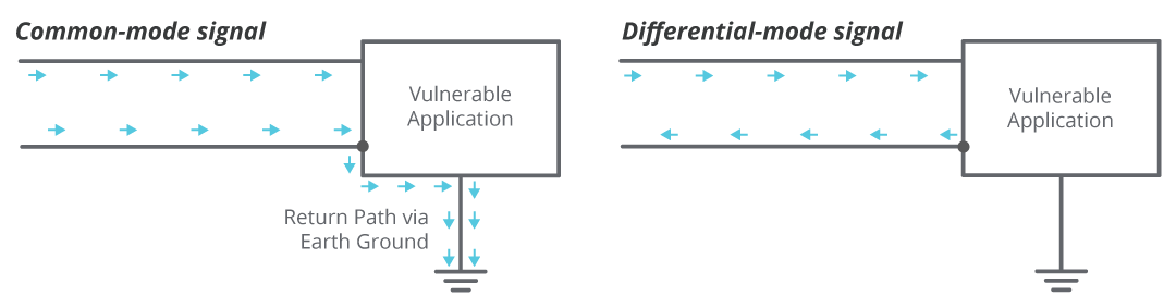
Conducted EMI emissions are measured up to 30 MHz. Currents at frequencies below 5 MHz are mostly differential mode, while those above 5 MHz are usually common mode.
Inductive coupling occurs where the source and receptor are separated by a short distance. Inductive coupling can be due to electrical induction or magnetic induction. Electrical induction results from capacitive coupling while magnetic induction is caused by inductive coupling. Capacitive coupling occurs when a varying electric field exists between two adjacent conductors, inducing a change in voltage across the gap. Magnetic coupling occurs when a varying magnetic field exists between two parallel conductors, inducing a change in voltage along the receiving conductor. Inductive coupling is rare relative to conductive or radiated coupling.
Radiated coupling occurs when source and receptor (victim) act as radio antennas. The source radiates an electromagnetic wave which propagates across the open space between the source and the victim and is received by the victim.
Characterization of the EMI problem requires understanding the interference source and signal, the coupling path to the victim and the nature of the victim, both electrically and in terms of the significance of the malfunction. The risk posed by the threat is usually statistical in nature; so much of the work in threat characterization and standards setting is based on reducing the probability of disruptive EMI to an acceptable level rather than its assured elimination.
EMI requirements, both radiated and conductive, apply to an overall electronic system. Power modules are one of many components within a system. Since the EMI requirements apply to the overall system, significant effort must be expended on system design to limit noise. Most electronic equipment has only one interface with the power source, which is through the power supply. If adequate EMI filters are inserted between the power supply and the power source, conducted emissions from the power module can be sufficiently suppressed to meet the FCC or CISPR limits without any of the power modules meeting the EMC standard as a standalone component. However, it should be noted that switching power supplies in stand-alone applications, typically in the form of external power adapters, are required to operate below the conducted EMI limits.
PRACTICAL MEASURES FOR EMI MITIGATION IN POWER SYSTEMS
In systems and circuits that are powered by switching power supplies, good practices should be observed in order to minimize EMI problems and ensure agency compliance. Suppression of EMI to levels below that specified by regulatory bodies requires an understanding of the design of the power supply and the application in which it is incorporated. It is important to note that even an application with a properly filtered switching power supply may not achieve compliance if the application is not designed to minimize EMI. Cautions must be taken to use the power supply/converter properly as intended, to prevent power supply generated noise from radiating or reaching the source, minimize noise pick up from the power supply, minimize system noise generation, and prevent system generated noise from reaching the power supply.
MITIGATION TECHNIQUES FOR CONDUCTED EMI
To effectively mitigate conducted emissions, it is imperative to address the differential mode noise and common mode noise separately because the remediation solution is different for each type of noise. Solutions for differential mode noise will not eliminate common mode noise present in the circuit. The same is true for common mode noise solutions as applied differential mode noise.
Differential mode noise can usually be suppressed by connecting bypass capacitors directly between the power and return lines of the power supply.
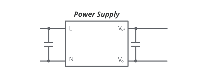
The power lines that require filtering may be those located at the input or the output of the power supply. The bypass capacitors on these lines need to be physically located adjacent to the terminals of the noise generating source to be most effective. The actual location of the bypass capacitor is critical for efficient attenuation of differential mode currents at high frequencies. Attenuation at lower frequencies of differential mode currents around the fundamental switching frequency of the noise generating source may dictate that a much higher value of bypass capacitance be required that cannot be attained with a ceramic style capacitor. Ceramic capacitors up to 22 µF may be suitable for differential mode filtering across the lower voltage outputs of switching power supplies but not suitable for inputs where 100 volt surges can be experienced. For these applications electrolytic capacitors are employed because of their high capacitance and voltage ratings.
Differential mode input filters usually consist of a combination of electrolytic and ceramic capacitors to suitably attenuate differential mode current both at the lower fundamental switching frequency as well as at the higher harmonic frequencies. Further suppression of differential mode currents can be achieved by adding an inductor in series with the main power feed to form a single stage L-C differential mode low pass filter with the bypass capacitor.
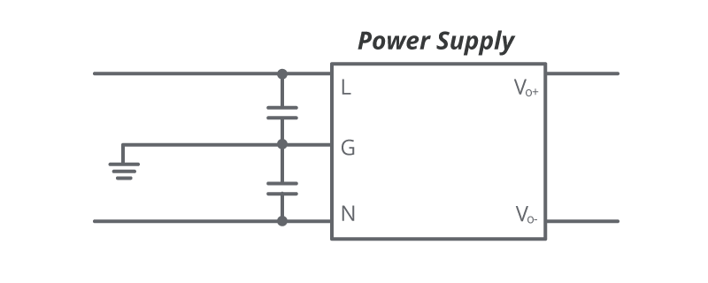
Common mode conducted currents are effectively suppressed by connecting bypass capacitors between each power line of the supply and ground. These power lines may be at the input and/or at the output of the power supply. Further suppression of common mode currents can be achieved by adding a pair of coupled choke inductors in series with each main power feed. The high impedance of the coupled choke inductors to exiting common mode currents forces those currents through the bypass capacitors.
MITIGATION TECHNIQUES FOR RADIATED EMI
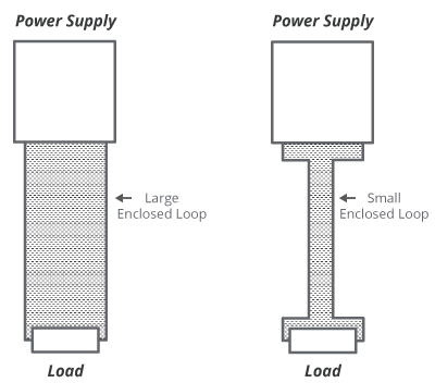
Radiated EMI can be suppressed by reducing RF impedance and reducing the antenna loop area which is done by minimizing the enclosed loop area formed by the power line and its return path. The inductance of a printed circuit board track can be minimized by making it as wide as possible and routing it parallel to its return path. Similarly, because the impedance of a wire loop is proportional to its area, reducing the area between the power line and its return path will further reduce its impedance. Within printed circuit boards this area can be best reduced by placing the power line and return path one above the other on adjacent printed circuit board layers. Recall that reducing the loop area between a power line and its return path not only reduces the RF impedance, but also reduces the effectiveness of the antenna because the smaller loop area produces a reduced electromagnetic field. A ground plane located on the outer surfaces of the printed circuit board, particularly if located directly below the noise generating source, suppresses radiated EMI significantly.
To further reduce radiated noise, metal shielding can be utilized to contain radiation. This is achieved by placing the noise generating source within a grounded conductive housing. Interface to the clean outside environment is via in-line filters. Common mode bypass capacitors would also need to be returned to ground on the conductive housing.
ADDITIONAL MITIGATION CONSIDERATIONS FOR SWITCHING POWER SUPPLIES
Reliable wiring connections should be implemented to and from the power supply. Wiring must be of suitable size and be kept as short as possible, and wiring loops should be minimized. Avoid running input or output wirings near power devices to prevent noise pick up.
Ensure all grounding connections are made and properly secured. Earth ground wires should be kept as short as possible. If the circuit or system operations induce current transients, it is very important to have local decoupling capacitors to supply the pulsed current locally, instead of letting the pulsed current propagate upstream to the supply. These capacitors should include high frequency ceramic caps and bulk capacitors. If the operation allows, slow down the clock, or rising/falling edges. Circuits with higher clock rates/fast switching times should be located close to the power line input to reduce power transients. It is recommended that both analog and digital circuits should be individually physically isolated on both power supply and signal lines.
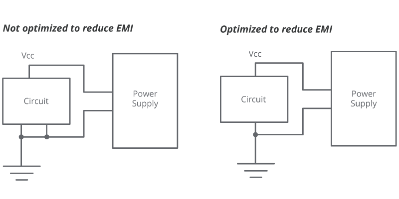
Care must be taken to prevent ground loops in the system, especially when the system becomes complex. This can be achieved by using a single point ground or a ground plane. An example is highlighted in figure 7.
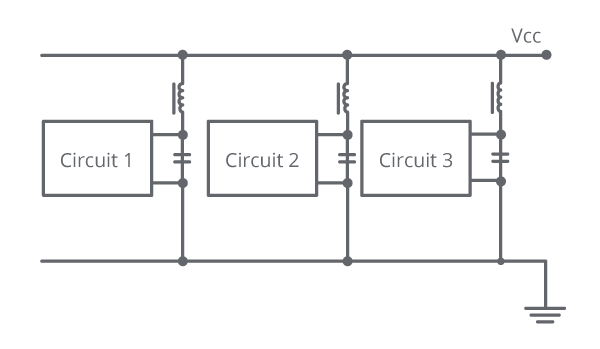
If there are multiple circuits in a system, decouple the circuits from each other by running separate supply lines, and/or place inductance in the supply lines as highlighted in figure 8 below.
If needed, ferrite beads can be placed on the dc supply lines to isolate the system and the supply. This can be effective to prevent power switching harmonics from disrupting the system’s operation, or to prevent system generated noise from reaching the power supply. On the input side, if the built-in EMI filter is insufficient for a specific application, additional EMI filtering can be applied before the power supply. A bead can also be placed on the earth ground wire between the ac inlet and the supply.
Although many of the mitigation techniques highlighted above are applicable to the implementation of both ac-dc and dc-dc converters within a system, there are specific considerations that must be addressed for dc-dc converters. The switching action in most dc-dc converters demand a pulsed input current, which is best supplied by local capacitors close to the switching devices.
As many dc-dc converters are compact in size, they generally do not contain sufficient capacitance. The system designer will need to place additional capacitance at the input to reduce differential mode noise. For even better filtering performance, a PI filter can be employed. The additional capacitors are used to reduce common mode noise.
ADDITIONAL SYSTEM-LEVEL MITIGATION TECHNIQUES
As mentioned above, although most switching power supplies are designed to meet applicable EMI standards as stand-alone modules, the system itself needs be designed to generate a minimum EMI profile to meet regulatory standards. Specific areas in the system design that are candidates for EMI mitigation practices include the signal lines, printed circuit boards (PCB), and solid state components.
Signal line considerations include the use of low pass filters on signal lines to reduce allowable bandwidth on the line to the minimum that will still allow the signal to pass un-attenuated. Feed and return loops should be kept close on wide bandwidth signal lines to minimize radiated emissions. Additionally, signal lines carrying RF or near-RF signals should be properly terminated to reduce reflection at the termination. Ringing and overshoot on these lines can also be minimized as a result of using the appropriate termination.
PCB high impedance runs that contribute to EMI can be mitigated by using wide PCB metal stripes to decrease the impedance of power lines. Where possible, signal tracks should be designed considering their propagation delay vs. signal rise/fall time and include a ground and a power plane. Slit apertures in PCB layout should be strictly avoided, particularly in ground planes or near current paths to reduce unwanted antenna effects. Board metal stripes should be kept as short as is practical, and metal stubs which can cause reflection and harmonics should be avoided.
Also, avoid overlapping power planes to reduce system noise and power coupling. Reduce or eliminate sharp bends in metal stripes (also known as beveling or track mitering) to reduce field concentration and run conducting stripes orthogonally between adjacent layers to reduce crosstalk. Floating conductor areas can act as a source of radiated emissions, so their use should be avoided except for overriding thermal considerations. Additionally, solid state components on the PCB should be decoupled close to chip supply lines to reduce component noise and power line transients.
SUMMARY
Switching power supplies can generate EMI because of their inherent design. Domestic and international regulatory bodies regulate these emissions through promulgation of rules and standards such as the FCC Part 15 rules and the CISPR 22 standard.
Noise has been discussed with respect to type, how the noise is transmitted, frequency of the noise, and noise modes in circuits. A basic design guideline for suppression of noise has been provided, including input/output filter circuits and reduction of antenna loop area. Best practices for EMI mitigation as regards power supply, signal line, printed circuit board (PCB) and components have also been discussed.