EMI Filter Components: what they are and how they work
August 2, 2022 by Bruce Rose - 10 Minute Read
Power Supply Block Diagram
It has come to the time in your project where you need to select the internal ac-dc and dc-dc power supplies. On the last project you selected supplies with internal EMI and EMC components, but on this project the supplies you are looking at require external EMI and EMC components. In this discussion we will help you to understand why the different components are needed and how they should be selected. We will not cover the details of EMI and EMC, the basic concepts are ‘do no harm to other systems’ and ‘operate properly in the presence of outside electrical disturbances’. A more detailed discussion of EMI and EMC can be found on this web page: What is the Difference Between EMI and EMC in Power Supplies?.
The block diagram of a power supply in Figure 1 was presented and discussed in a previous web article, How Switch Mode Power Supplies Work, Block by Block, and will be used as the basis for this discussion.
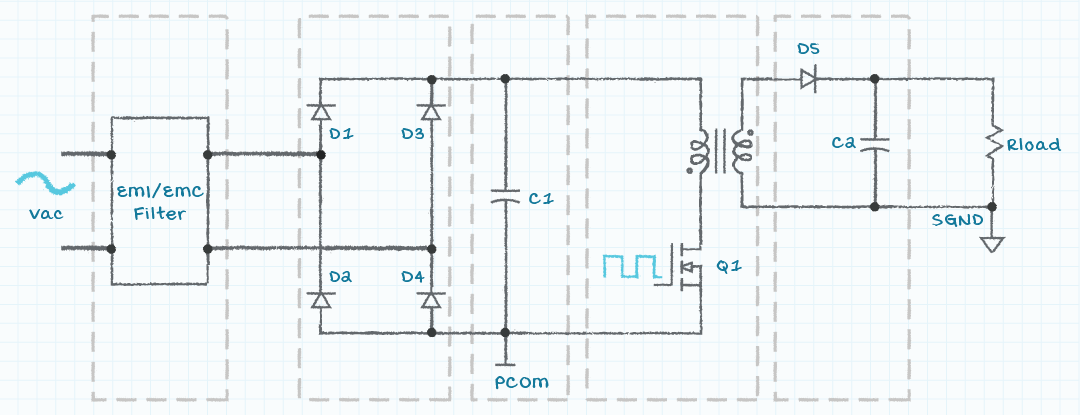
In the diagram above the EMI/EMC filter is shown as a block at the input to the power supply. In practice, as shown in Figure 2 below, some of the EMI/EMC filter components are placed on the input of the power supply, some are placed on the output of the power supply, and some are placed between the input and the output of the power supply.
The EMI/EMC components may be utilized to serve the following functions:
- Minimize radiated and conducted noise on the input or output of the power supply
- Minimize the effects of voltage transients applied to the input or output of the power supply
- Minimize the input surge current when voltage is first applied to the input of the power supply
- Protect the input power source and conductors if there is a failure of the power supply
Circuit Protection Components
Fuse
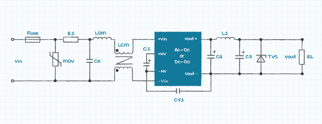
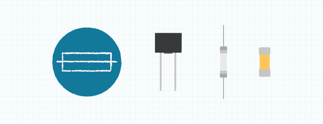
The fuse is present to protect the power source and conductors feeding into the power supply and is placed in series with the input of the power supply. For reasons of protection, there should be no components between the fuse and the conductors from the upstream power source. The fuse should be placed in series with the non-ground input terminal so that if the fuse opens, there is no voltage present on the power supply. If the properly sized fuse has been opened by excessive input current into the downstream power supply, the fuse should not just be replaced but the downstream power supply is damaged and should be repaired or replaced. The fuse should be selected based upon the voltage, current, response time and operating temperature of the application. There are also a range of package options to choose from, such as those shown in figure 3, which can help further optimize the design.
Metal Oxide Varistor (MOV)
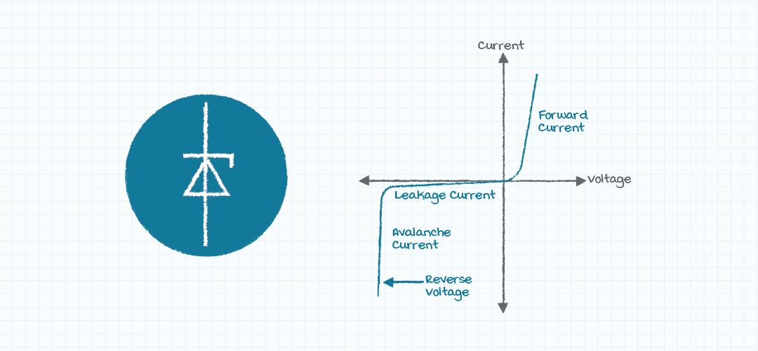
The Metal Oxide Varistor (MOV) is placed in across the input terminals and is included to absorb voltage transients which may come from the input voltage source. In the case of an ac-dc power supply, the input voltage source is the ac power lines and the MOV may be required to absorb transient energy from lighting strikes or other damage to the ac power network. A MOV component is a high impedance during normal operation and becomes a low impedance when the rated voltage is exceeded, as would happen when an input transient voltage is present. An input fuse should always be placed between the MOV and the input power source. The fuse may be blown if the MOV goes to low impedance due to a transient input voltage. The MOV should be selected based upon the operating voltage and transient energy which may be applied to the power supply. Alternative protection components to a MOV might be a Zener, TVS (Transient Voltage Suppression) diode or a GDT (Gas Discharge Tube).
Input Surge Current Limiting Resistor
The resistor labeled R1 in the diagram of the EMI/EMC components applies to ac-dc power supplies and is included to limit the input surge current when ac voltage is first applied to the power supply. The input surge current is due to the initial rapid charging of the bulk capacitor when the input voltage is first applied. Without a current limiting resistor, the input surge current may be as much as 100 times greater than the normal operating current. A higher value of current limiting resistor reduces the input surge current but may create unacceptable power losses during normal operation. Care should be exercised when choosing the construction of the input surge current resistor. The resistor must be able to tolerate the high energy burst when the input surge current is flowing. Wire wound construction resistors are often a good choice for the input surge current limiting resistor. Film construction resistors typically are not suitable to handle the large input surge energy.

In some designs a negative temperature coefficient (NTC) resistor is used for the input surge current limiting resistor. The NTC resistor has a high resistance value when it is cold and effectively limits the input surge current. When the NTC resistor heats up, due to the flow of input current, the value of the resistance drops and thus the associated power dissipation by the resistor also drops. The NTC resistor should be allowed sufficient time (tens of seconds) to cool down and return to a high impedance value when the power supply is shut down and before the input power is reapplied. Many dc-dc converter applications do not require an input surge current limiting resistor. The input surge current may be inherently limited if the input voltage is relatively low (peak input voltage for 240 Vac is 340 V) or the source impedance of the input supply will limit the maximum available input current.
Output Transient Voltage Suppression
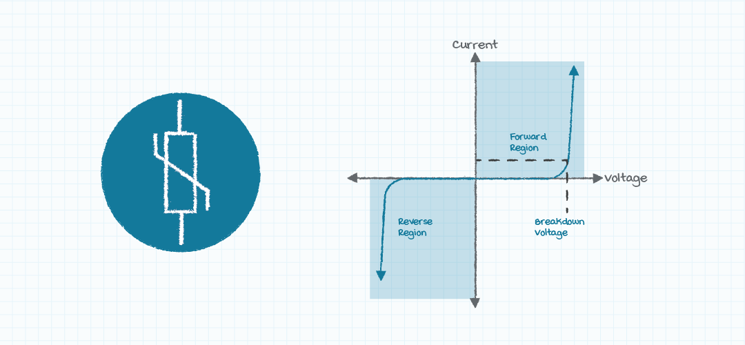
The TVS (Transient Voltage Suppression) diode on the output of the supply can serve two different purposes. A common reason for including the TVS diode on the output of the power supply is to shunt voltage transients induced by external sources on the output terminals of the power supply and thus protect the power supply. While a MOV is often used for a similar purpose on the input of the power supply, the voltage across the output of the power supply and the energy associated with induced transients on the output of the power supply are both often lower than on the input and thus a TVS diode is a more appropriate solution. A Zener diode can be used in place of the TVS diode if there is also a desire to clamp the output voltage in the event of a failure of the output of the power supply. It should be noted that in this situation the power required to be dissipated by the Zener diode may be greater than the output power rating of the power supply. The Zener diode will have a breakdown voltage greater than the power supply output voltage and during the failure the power supply will probably be able to deliver greater than the rated output current.
EMI Filter Components
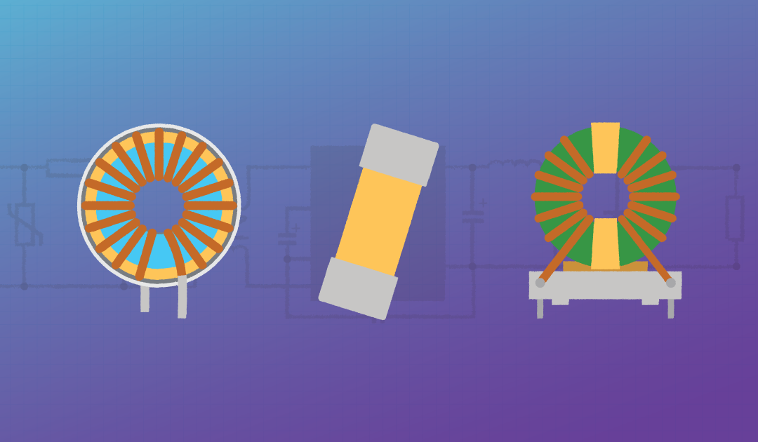
Differential Mode Choke
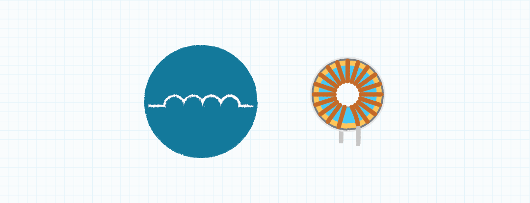
The inductor labeled LDM is placed in series with the input power path. This component forms a low-pass LC filter with the input capacitor, CX, to attenuate the undesired conducted noise voltage on the input conductors from reaching the external power source. The saturation current specification for this inductor must be great enough to tolerate the maximum input current during normal operation. It is acceptable if the inductor saturates during the inrush start-up current surge. The differential mode inductor should be selected with sufficiently low DCR (parasitic dc resistance) so the power dissipation of the inductor is acceptable.
Common Mode Choke
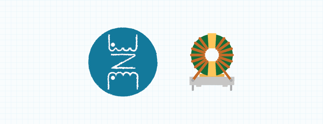
The double-winding choke labeled LCM is an input common mode choke. The common mode choke serves to create a high impedance to attenuate common mode currents flowing along the input conductors. Care should be taken when placing the common mode choke in the schematic to ensure the orientation of the ‘dots’ is correct. The dots indicate the relative winding direction for the pair of windings. It is not important whether the dots are on the input or the output of the connections to the common mode choke, but both dots should be on the same electrical side of the choke. The differential mode choke does not require dot notation; there is only one winding and the direction of current flow does not matter. The common mode choke should be chosen to handle the maximum current flow during normal operation of the power supply and to have acceptable power dissipation during normal operation of the power supply. Unlike the differential mode choke, the common mode choke has very little current flowing in common mode and thus the saturation current rating is normally not an issue.
X Safety Class Input Capacitor
The capacitor labeled CX, which is placed across the input power lines, serves to shunt differential conducted voltage noise so the noise does not continue to the external voltage source. This capacitor should be of X or Y safety class construction. Both X and Y safety class capacitors are designed to be connected directly to the ac input lines and thus can tolerate the voltage surges which may be present. A larger value of capacitance serves as a lower impedance to better shunt the undesired noise, but it will also increase the input leakage current in an ac-dc power supply. Many ac powered systems are required to meet regulatory standards, which may include maximum input leakage current limits and thus will limit the amount of capacitance in the shunt capacitor.
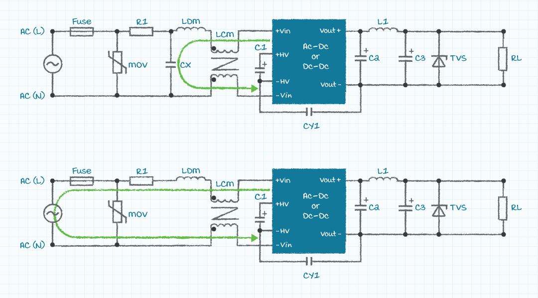
Y Safety Class Isolation Capacitor
The capacitor placed between the input and the output and labeled CY1 in the schematic diagram serves to attenuate common mode voltage noise on the output of the power supply. This capacitor is selected to be Safety Class Y since it is across the isolation barrier. Safety Class Y capacitors are designed to fail as an open circuit and thus the integrity of the input to output isolation of the power supply is maintained in the event of a failure of the capacitor. In some applications two capacitors are required to be placed in series to provide even greater assurance of the integrity of the isolation between the input and the output of the power supply.
The need for capacitor CY1 is due to the voltage waveform caused by the primary side switching transistor, and the parasitic capacitance between the primary and secondary side of the isolation magnetics (figure 9). Capacitor CY1 should be placed between the source of the primary side switching FET and the terminals of the secondary winding of the isolation magnetics. As will soon be discussed, the output terminals of the isolation magnetics have large value bypass capacitors between them and thus are at the same ac potential. Therefore, the output terminal of capacitor CY1 can be connected to either output terminal. The value of the capacitance of CY1 is selected to be significantly larger than the value of the primary to secondary parasitic capacitance to provide acceptable attenuation of the common mode voltage on the output of the power supply. It should be noted that a larger value of capacitor CY1 has the detrimental effect of causing greater ac leakage current between the input and the output of the power supply.

Input Bulk Capacitor
The capacitor labeled C1 in the schematic diagram is placed directly across the input of a dc-dc converter and after the bridge rectifier (and power factor correction circuit if present) in an ac-dc supply. In a dc-dc converter this capacitor serves as an input charge reservoir to attenuate input voltage disturbances due to input current transients. The purpose of this capacitor in an ac-dc supply is to filter the rectified ac input voltage and provide energy to sustain the output voltage when the ac input voltage is removed. The previously discussed input surge current limiting resistor is used to limit the maximum current drawn when this capacitor is initially charged
Output Filtering
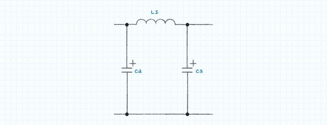
The filter components placed on the output terminals of the power supply can be used to address EMI and EMC issues, but they are often placed near the load and the component values are selected to reduce the output ripple voltage to a level that is acceptable for the load. For simplicity, many power supply applications replace L1 with a short circuit. As was stated earlier, capacitor C2 provides a low impedance ac path between the power supply output terminals and thus allows CY1 to be connected to either output terminal of the power supply.
EMC Component Selection
By now it is probably obvious that selecting proper components to prevent EMI and EMC issues associated with power supplies is not difficult but there are many details to consider. Often the final choice of components and component values is a compromise between performance, cost, size, and power conversion efficiency. Most power supply vendors, such as CUI, have customer support engineers who are willing to provide additional assistance if you should require it during the course of your project.
Fundamentals , Safety & Compliance
Have comments regarding this post or topics that you would like to see us cover in the future?
Send us an email at powerblog@cui.com


Bruce Rose
During his many years in the electronics industry working in design, sales, and marketing, Bruce Rose has focused on analog circuits and power delivery. His range of work experience includes organizing and chairing international workshops, publishing and presenting in more than 40 technical conferences and journals, and having been awarded seven patents. While he enjoys his time at work, Bruce further enjoys the time he is able to spend with his family hiking, biking, and canoeing as well as pursuing his passion of full scale and model aviation.