EMI Solutions for External Power Supplies
December 17, 2019 by Bruce Rose - 7 Minute Read
Management may ask their engineering team, "Why is conducted or radiated emissions testing required on the system when the external power supply already meets regulatory requirements?" A simple answer is that the power supply development team tested the supply in isolation and the radiated and conducted emissions characteristics will be different when the complete system is tested. This post will discuss how ferrite beads can be used to bring systems comprised of an external supply and the system load into regulatory compliance regarding conducted and radiated emissions.
Conducted and Radiated Emissions
Electronic products typically have at least two types of signals associated with them. One category of signals is the intended signals; power and data. Unfortunately, intentional voltage transitions in the power and data signals give rise to a second type of signal in electronic products; unintended noise.
Regulatory agencies have placed limits on the levels of noise signals that are allowed to be propagated outside of the system. Two of the more common regulations regarding electronic emissions are the US standard FCC Title 47, Part 15 and the European standard EN55022. The dominant means of propagation of the noise depends upon the frequency band of the noise.
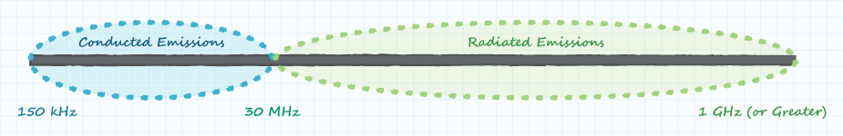
Most low frequency electromagnetic noise is propagated by conduction. For the purposes of regulatory issues, the range of ‘low frequency' electromagnetic signals is considered to be 150 kHz to 30 MHz. The conductors within the system are typically too short to serve as effective antennas in this frequency range and thus radiated emissions are not a major concern. Within this frequency band, the impedance of parasitic inductors is low enough and the impedance of parasitic capacitors is high enough such that the signals can be propagated along conductors without significant attenuation. For high frequency electromagnetic signals (30 MHz and above), the parasitic impedances associated with conductors can create significant attenuation to conducted signals. However, conductors in electronic products can be long enough to serve as reasonable antennas at those frequencies and thus radiation is the primary emission concern at the higher frequencies.
Filters to Address Conducted and Radiated Emissions
External power supplies typically incorporate discrete inductors and capacitors in the AC input circuitry to attenuate noise from being conducted out from the power supply along the AC input power lines. The internal PCB is designed to accommodate these components and regulatory safety testing is performed with the components installed. Once the design and testing activities have been completed, changes to the input filter elements to accommodate customer needs are normally prohibitively expensive.
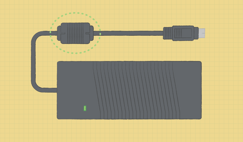
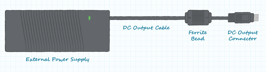
The DC output circuits in external power supplies employ internal shunt capacitors to attenuate AC signals on the output of the power supply. Some designs may also include series inductors to provide additional attenuation of the AC signals. However, during final radiated emissions testing it may be observed that the internal filtering is not sufficient to meet the regulatory requirements for emissions. The DC output cable is not monitored for conducted emissions but may serve as a reasonable antenna for radiated emissions. One solution to address excessive radiated emissions is to add an external ferrite bead on the DC output cable to bring the supply into compliance. The ferrite beads used for EMI filtering are designed to provide both a reactive and a resistive impedance. The reactive impedance helps to block the propagation of undesired signals while the resistive impedance dissipates some of the energy associated with the undesired signals. The bead is selected to physically fit around the DC output cable and to provide the necessary filtering characteristics at the frequencies of concern.

Ferrite Bead Filters Added During System Testing
A power supply is tested in isolation by the power supply design team to meet conducted and radiated emission requirements. However, once the power supply is added to a complete system, the system may fail similar emissions testing. One of the common reasons for the failure of the complete system is noise from the system load propagating through the DC output power cable back to the power supply. The addition of ferrite beads on the DC output cable is a low cost solution that may be able to reduce the emissions to an acceptable level.
Selecting Ferrite Beads and Transitioning to Production
- Test the system and the external power supply to determine if frequencies exist at which excessive emissions occur.
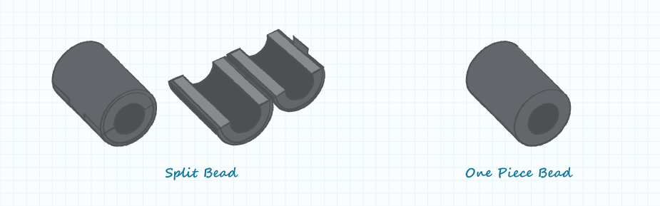
- Select a ferrite bead which will physically fit around the cable and will provide high impedance at the frequencies of concern. Some ferrite bead companies provide split ferrite beads for testing and low volume manufacturing purposes. Split ferrite beads allow assembly onto the cable without requiring the DC output connector to pass through the hole in the ferrite bead.
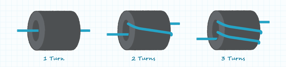
- Install the ferrite bead. Often the ferrite bead is placed at the DC connector end of the cable to reduce noise signals before they are transmitted along the cable from the system load to the power supply. Typically, two turns of the cable are placed through the ferrite bead. The impedance provided by the bead is approximately proportional to the number of turns squared; two turns provides four times the impedance of a single turn. When implementing more than two turns, the series impedance per turn rises to a high enough level that the parasitic capacitance between the cable segments shunt energy past the series impedance created by the bead. The shunting of the undesired signals through the parasitic capacitance reduces the effectiveness of the ferrite bead to less than would be if only two turns were employed.
- If the product will be placed in volume manufacturing, select a non-split ferrite bead comparable in specifications to the bead used in testing. The vendor for the ferrite bead used in production may be different than that of the bead used for testing.
- Construct samples of the power supply with the ferrite bead to be used in volume production.
- Test the system and the external power supply with the ferrite bead used for production installed on the power supply DC output cable. This re-testing ensures that the combination of the power supply, production ferrite bead, and system meet emissions requirements.
Summary
When power supplies and system loads are combined, the system design team sometimes encounters issues with the overall system not meeting conducted and radiated emissions requirements. Often changing the design of the power supply or of the system load will be prohibitively expensive, both in schedule time and resource costs. Ferrite beads (designed with inductive and resistive impedance components) placed on the power supply DC output cable can be used to enable the overall system to meet conducted and radiated emissions requirements. Selecting the proper bead is a multi-step process and may require coordination between the system design team and the manufacturer of the power supply.
You May Also Like

Have comments regarding this post or topics that you would like to see us cover in the future?
Send us an email at powerblog@cui.com


Bruce Rose
During his many years in the electronics industry working in design, sales, and marketing, Bruce Rose has focused on analog circuits and power delivery. His range of work experience includes organizing and chairing international workshops, publishing and presenting in more than 40 technical conferences and journals, and having been awarded seven patents. While he enjoys his time at work, Bruce further enjoys the time he is able to spend with his family hiking, biking, and canoeing as well as pursuing his passion of full scale and model aviation.