
How to Select a Heat Sink
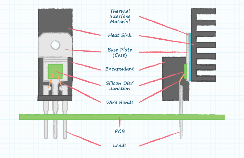
Heat sinks are an important element in circuit design because they provide an efficient path for heat to be transferred into the ambient air and away from electronic devices (eg. BJTs, MOSFETs, linear regulators, BGA packages, etc.). The general theory behind a heat sink is to increase the surface area of the heat-producing device, enabling a more efficient transfer of heat into the ambient environment. This improved thermal pathway reduces the temperature rise in the junction of the electronic device. The following post is intended to provide high-level primer on heat sink selection utilizing thermal data from your application and specifications from the heat sink vendor.
Is a Heat Sink Required?
For the remainder of this post, let us assume that an application is being developed using a transistor housed in a TO-220 package, the switching and conduction losses of the transistor equate to a power dissipation of 2.78 W, and the ambient operating temperature of this application is not expected to exceed 50°C. Will a heat sink be required for this transistor?
The first step is to gather and understand all of the thermal impedances that stand in the way of the 2.78 W from being dissipated into the ambient air. If those Watts cannot dissipate efficiently, the junction temperature inside the TO-220 package will rise beyond the recommended operating conditions (typically 125°C for silicon).
Most transistor vendors will document a “junction-to-ambient” thermal impedance denoted by the symbol Rθ J-A, which is measured in units of °C/W. This value represents how much the junction temperature will rise above the ambient temperature surrounding the TO-220 package for every Watt of power dissipated within the device.
For example, if the transistor vendor states that the thermal impedance from junction-to-ambient is 62°C/W, this means that the 2.78 W being dissipated within the TO-220 package will cause the junction temperature to rise 172°C above ambient (calculated as 2.78 W x 62°C/W). Assuming the worst-case ambient temperature for this application of 50°C, the junction temperature will reach 222°C (calculated as 50°C + 172°C). This far exceeds the rated silicon temperature of 125°C and will permanently damage the transistor. Hence, a heat sink is required. Attaching a heat sink will lower the junction-to-ambient thermal impedance significantly. The next step will be to determine how low the thermal impedance path needs to be for safe and reliable operation.
Determining Thermal Impedance Paths
To do this, start with the largest permissible temperature rise. If the maximum ambient operating temperature of the application is 50°C and the silicon junction must remain at 125°C or less, the largest permissible temperature rise is 75°C (calculated as 125°C - 50°C).
Next, calculate the largest permissible thermal impedance between the junction and ambient air. If the largest permissible temperature rise is 75°C and the Watts dissipated in the TO-220 package is 2.78 W, the largest permissible thermal impedance would be 27°C/W (calculated as 75°C ÷ 2.78 W).
Finally, add up all the thermal impedance paths from the silicon junction to the ambient air and ensure they sum up to less than the largest permissible thermal impedance; 27°C/W in this example.
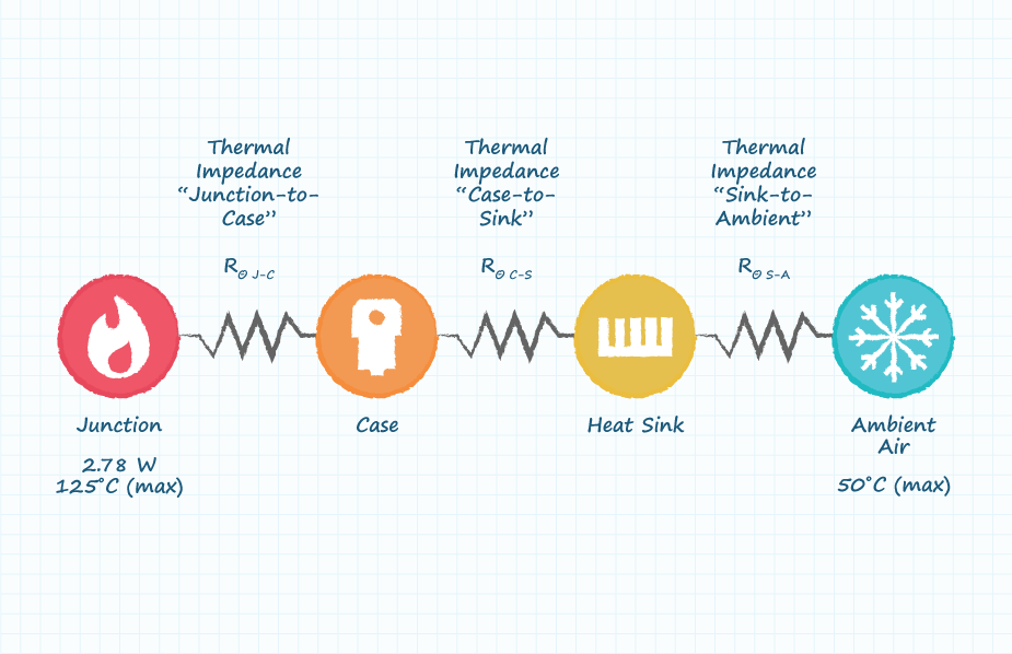
From the figure above, the first thermal impedance required is “junction-to-case” denoted by the symbol Rθ J-C. This is a measure of how easily heat can be transferred from the junction, where the heat is being generated, out to the surface (case) of the device (TO-220 in this example). Most vendors will list this impedance in their datasheet alongside the junction-to-ambient metric. For this example, the assumed junction-to-case thermal impedance is 0.5°C/W.
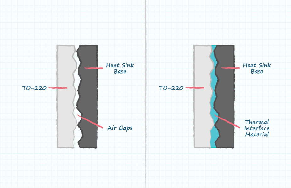
The second thermal impedance required is “case-to-sink” denoted by the symbol Rθ C-S This is a measure of how easily heat can be transferred from the surface (case) of the device to the surface of the heat sink. Due to irregularities in the surfaces of the TO-220 case and heat sink base, it is generally recommended to use a Thermal Interface Material (TIM or “thermal compound”) between the two surfaces to ensure that they are fully engaged from a thermal perspective. This greatly improves the transfer of heat from the TO-220 case to the heat sink, but does have a thermal impedance associated with it that must be taken into account.
Accounting for Thermal Interface Materials
Thermal Interface Materials (TIMs) are typically characterized by their thermal conductivity in terms of Watts per Meters-Celsius (W/(m °C)) or Watts per Meters-Kelvin (W/(m K)). Celsius and Kelvin are interchangeable in this example because they both use the same increment of temperature measurement and it is the rise/fall of temperature that is being calculated (eg. a 45°C rise in temperature is equivalent to a 45 K rise in temperature). The unit of meters is present because the impedance of the TIM is dependent upon the ratio of thickness (the thickness of the TIM material in terms of meters) over area (the area which the TIM is spread over in terms of meters2), which results in 1/m (calculated as m/m2 = 1/m). We discuss TIMs in greater detail in our The Importance of Thermal Interface Materials blog. In this example, a thin layer of TIM will be applied over the metal tab area of a TO-220 case. Here are the specific TIM properties and application details used in this example:
TIM’s thermal conductivity ("K"): 0.79 W/(m °C) = 0.79 W/(m K)
TIM’s area of application: 112 mm2 = 0.000112 m2
TIM’s thickness of application: 0.04 mm = 0.00004 m
The thermal impedance of the TIM can be calculated from the properties listed above using the following equation (note the use of meters for unit consistency):
Rθ C-S = (Thickness / Area) x (1 / Conductivity)
Rθ C-S = (0.00004 / 0.000112) x (1 / 0.79)
Rθ C-S = 0.45 C/W or 0.45 K/W
Selecting the Heat Sink
The final thermal impedance required is “sink-to-ambient” denoted by the symbol Rθ S-A. This is a measure of how easily heat can be transferred from the base of the heat sink to the ambient air. Heat sink vendors like CUI Devices will typically provide graphs like the one below or data points to illustrate how easily heat can be transferred from the heat sink to the ambient air under various airflow conditions and loads.
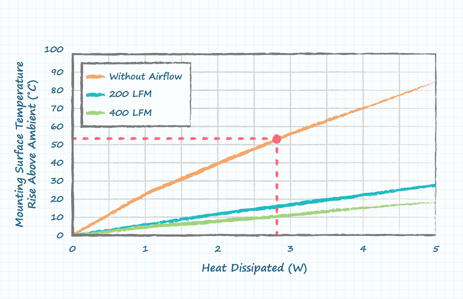
For this example it is assumed that the application is operating under natural convection conditions without any airflow. The graph above can be used to calculate the final thermal impedance (sink-to-ambient) for this particular heat sink. The surface temperature rise above ambient divided by the heat dissipated provides thermal impedance at that specific operating condition. In this example the heat dissipated is 2.78 W, which results in a surface temperature rise above ambient of 53°C. Dividing 53°C by 2.78 W produces a sink-to-ambient thermal impedance of 19.1°C/W (calculated as 53°C ÷ 2.78 W).
In prior calculations, the maximum impedance allowed between the junction and ambient air was 27°C/W. Subtracting the impedance of the junction-to-case (0.5°C/W) and the impedance of the case-to-sink (0.45°C/W), the maximum allowance left over for the heat sink is 26.05°C/W (calculated as 27°C/W - 0.5°C/W - 0.45°C/W). The thermal impedance of 19.1°C/W for this heat sink under the assumed conditions is well below the previously-calculated allowance of 26.05°C/W. This translates to a cooler silicon junction temperature inside the TO-220 package and more thermal margin in the design. The maximum temperature of the junction can be estimated by adding up all the thermal impedances, multiplying them by the number of Watts dissipated in the junction, and adding the result to the maximum ambient temperature:
Estimated Junction Temp. = TAmbient + Watts x ( RθJ-C + Rθ C-S + Rθ S-A)
Estimated Junction Temp. = 50 + 2.78 x ( 0.5 + 0.45 + 19.1)
Estimated Junction Temp. = 105.7°C
The Importance of Heat Sinks
Heat sinks are an important element in thermal management as evidenced in this example. Without the heat sink, the silicon junction inside the TO-220 package would have far exceeded the rated limit of 125°C. The process used in this example can easily be modified and repeated to aid designers in selecting properly sized heat sinks for a myriad of different applications.
Key Takeaways
- Heat sinks are an important element in circuit design because they provide an efficient path for heat to be transferred into the ambient air and away from electronic devices.
- Defining the maximum temperature of the ambient environment and the power dissipated within the application will help to optimize the heat sink selection; not too small causing burnout and not too big wasting money.
- Thermal Interface Materials (TIMs) play an important role in transferring heat more efficiently and consistently between two surfaces.
- Once the parameters of the application have been defined (e.g. ambient temperature, power dissipation, thermal impedance paths, etc.), CUI Devices' product search filters can assist in finding just the right board level or BGA heat sink for the job.

 Tags:
Tags:
Additional Resources