How Gallium Nitride (GaN) Enables Smaller, More Efficient Power Supplies
January 7, 2020 by Ron Stull - 5 Minute Read
What is GaN?
Gallium Nitride (GaN) is a wide band-gap (WBG) semiconductor material. Like silicon, GaN can be used to make semiconductor devices such as diodes and transistors. The development of GaN transistors has been of particular interest to the power electronics industry as a replacement to silicon transistors. As a transistor, GaN shows significant advantages over silicon in key areas that allow power supply manufacturers to significantly increase efficiency, while at the same time decreasing the size and weight of their devices.
How Does GaN Improve Efficiency?
Power transistors are one of the primary contributors to power loss in a switching power supply. Losses in the transistors are generally separated into two categories; conduction and switching. Conduction losses are those caused by current flow when the transistor is on and switching losses occur in the transition between on and off states.
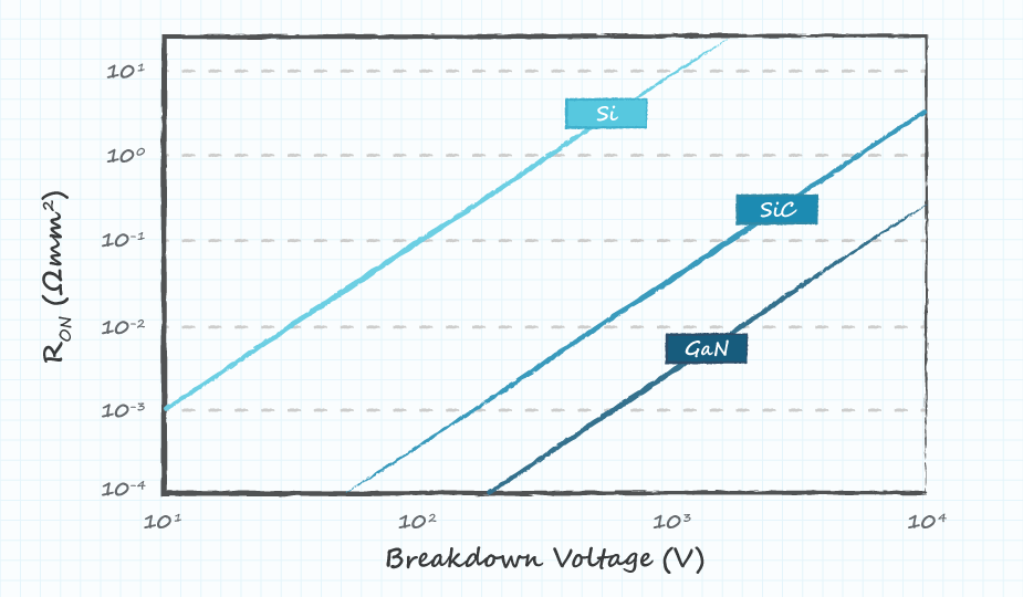
When on, GaN transistors (like those made of silicon) resemble a resistance between drain and source, often referred to as Ron, and the conduction losses are proportional to this resistance. A key benefit of GaN and other WBG materials is their relationship between breakdown voltage and Ron. Figure 1 shows the theoretical limits of this relationship for silicon, GaN, and silicon carbide (SiC), another WBG material. It can be seen that for a given breakdown voltage, the Ron of the WBG devices is much lower than that of silicon, with GaN being the lowest of the three. As silicon is nearing its theoretical limit, the use of GaN and other WBG materials becomes necessary if improvements to Ron are to continue.
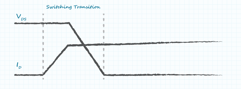
In addition to improvements in conduction losses, the use of GaN also leads to a reduction in switching losses. There are multiple factors that contribute to switching losses, several of which are improved through the use of GaN. One loss mechanism results from the fact that the current in a transistor begins to flow before the drain-source voltage begins to fall, as shown in Figure 2. During this time, the losses (equal to the volt-amp product) are very large. Increasing the speed at which the switch turns on will reduce the losses incurred during this transition. Because GaN transistors are able to turn on faster than silicon transistors, they are able to reduce the losses caused by this transition.
Another way that GaN reduces switching loss is through the absence of a body diode. To avoid a short circuit condition, a period of time exists when both switches of a half-bridge are off, known as the ”dead-time”. During this period, current continues to flow, but because both switches are off, it is forced through the body diode. The body diode is much less efficient than the Ron resistance of a silicon transistor when it is on. For a GaN transistors there is no body diode. Current that would flow through the body diode of a silicon transistor instead flows through the Ron resistance. This significantly reduces the losses incurred during the dead-time.
Because the body diode of a silicon transistor conducts during the dead-time, it must be turned off when the other switch turns on. During this time, current flows in the reverse direction as the diode turns off, causing additional losses. In a GaN transistors, the absence of a body diode results in near zero reverse recovery losses.
How Does GaN Decrease Form Factor?
While switching losses occur in short periods within the switching period, it is useful to look at them averaged over time. While the losses during a single switching transition may be large, if the time period between switches is large (meaning a low switching frequency), the average value can be kept at a safe level. Because the switching losses are lower in GaN, the time between switches is able to be reduced, increasing the switching frequency. The increased switching frequency allows the size of many large components (such as the transformer, inductors, and output capacitors) to be reduced.
GaN and other WBG devices also have better thermal conductivity and can withstand higher temperatures than silicon. Both help to reduce the need for thermal management components such as bulky heatsinks, frames, or fans. The absence of these devices (along with the shrinking of the powertrain components mentioned earlier) all lead to significant reductions in the overall size of the power supply.
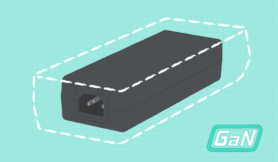
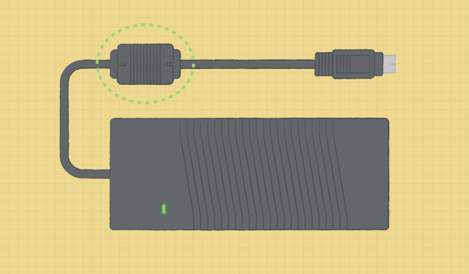
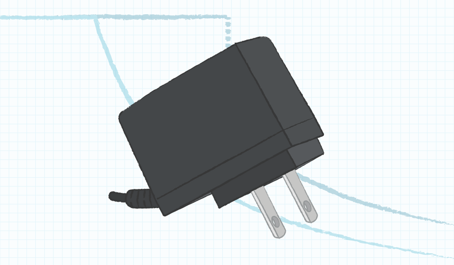
GaN Desktop Power Adapters
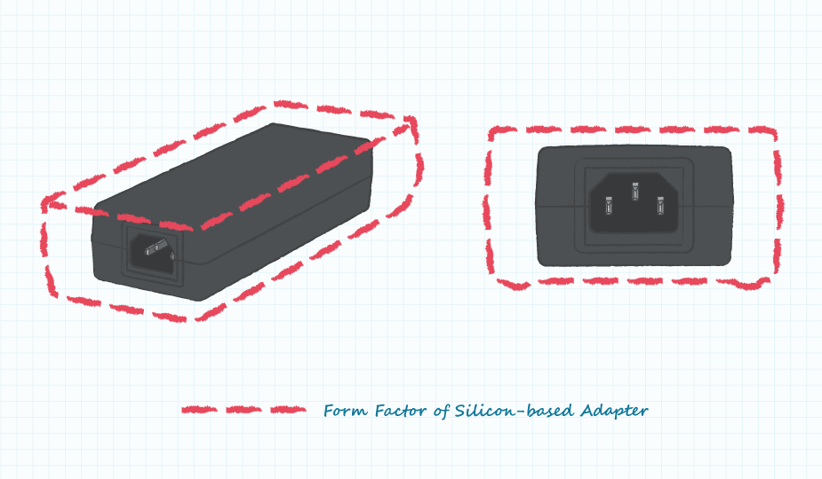
Improved efficiency, decreased size, and reduced weight have all been achieved, through the application of GaN, in CUI’s latest series of desktop adapters. For example, CUI’s SDI200G-U desktop adapter’s increased switching frequency has allowed its size to be reduced by more than half, increasing the power density from 5.3 W/in3 to 11.4 W/in3, which can be seen in Figure 3 below. This has also resulted in a weight reduction of 32% (820g to 560g). And by reducing conduction and switching losses, the adapters achieve efficiencies up to 95%. These GaN desktop adapters offer significant improvements to efficiency, size, and weight over conventional silicon-based supplies.
Conclusion
Power supply manufacturers are always seeking ways to increase the efficiency and power density of their products. Many of the gains over the years have come from improvements to the silicon switches used inside the power supplies. But as silicon reaches its physical limits, manufacturers have had to look elsewhere for improvements. The use of GaN (with its lower losses and faster switching) allows manufactures to push past the limitations of silicon and design smaller and more efficient power supplies while still leaving room to improve as GaN continues to develop. These improvements can be seen first-hand in CUI’s latest generation of GaN based adapters.
Industry News , Product Selection
You May Also Like


Have comments regarding this post or topics that you would like to see us cover in the future?
Send us an email at powerblog@cui.com


Ron Stull
Ron Stull has gathered a range of knowledge and experience in the areas of analog and digital power as well as ac-dc and dc-dc power conversion since joining CUI in 2009. He has played a key role on CUI’s Engineering team with responsibilities including application support, test and validation, and design. Outside of power engineering Ron can be found playing guitar, running, and touring the outdoors with his wife, where their goal is to visit all of the U.S. National Parks.